Market Overview and Introduction
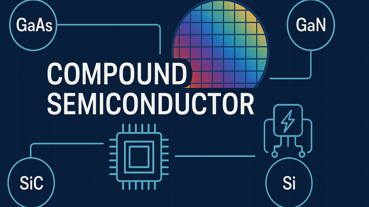
Accurately assessing the Compound Semiconductor Market Size reveals a story of profound economic significance and rapid transformation. The market, valued in the tens of billions of dollars, is on a trajectory to reach well over $100 billion within the next decade. This valuation reflects not only the growing unit shipments of devices like RF amplifiers, LEDs, and power transistors but also the increasing value per device due to the complex materials and advanced manufacturing processes involved. The market size is a composite measure, encompassing a diverse range of materials including Gallium Arsenide (GaAs), Gallium Nitride (GaN), and Silicon Carbide (SiC), each serving distinct high-value applications. The expansion of this market is a direct consequence of the global economy's increasing reliance on technologies that demand performance beyond the scope of traditional silicon. From the smartphones in our pockets to the infrastructure of the electric grid, the size of the compound semiconductor market serves as a key indicator of the world's progress toward a more connected, efficient, and electrified future.
Key Growth Drivers: Expanding the Addressable Market
The expansion of the market size is being propelled by a confluence of major technological shifts that are dramatically increasing the total addressable market (TAM) for compound semiconductors. The automotive sector is perhaps the most significant contributor. As electric vehicles (EVs) scale from a niche segment to mass-market adoption, the semiconductor content per vehicle is increasing exponentially. A single EV can contain hundreds of dollars' worth of compound semiconductor devices, primarily in the form of SiC MOSFETs and GaN power ICs. With global EV production projected to surge from millions to tens of millions of units annually, this alone creates a multi-billion dollar market expansion. Simultaneously, the global 5G rollout is a massive capital expenditure cycle. The 5G infrastructure market demands a much higher number of base stations and small cells than 4G, each packed with GaN and GaAs-based RF power amplifiers and front-end modules. This is supplemented by the 5G smartphone market, where the complexity and value of the RF front-end (which is increasingly GaAs-based) have grown significantly compared to 4G. Furthermore, the photonics market, driven by fiber-optic communication and high-speed data centers, relies on Indium Phosphide (InP) and Gallium Arsenide (GaAs) lasers and detectors, adding another substantial layer to the overall market valuation.
Consumer Behavior and E-commerce Influence
Consumer behavior acts as a powerful multiplier in expanding the market size by accelerating product replacement cycles and creating demand for premium, feature-rich devices. The consumer's appetite for the latest technology—the fastest 5G smartphone, the most powerful gaming laptop, the quickest EV charging capability—forces manufacturers to integrate higher-performing, and often more expensive, compound semiconductor components. This "upgrading" behavior increases the average selling price (ASP) of end devices, which in turn supports a larger total market value for its constituent components. E-commerce platforms are a critical vector for this behavior. They provide a global marketplace where new technologies, like GaN fast chargers, can achieve scale rapidly. The visibility and accessibility of these products on platforms like Amazon, Alibaba, and others enable quick consumer validation and mass adoption. The competitive nature of online sales, where product listings highlight key specifications, puts direct pressure on brands to continuously improve performance metrics—such as charging speed and power density—that are directly enabled by compound semiconductor technology. This dynamic feeds back into the market, increasing both the volume and value of components sold.
Regional Insights and Preferences: The Geography of Market Value
The distribution of the compound semiconductor market size is heavily skewed by regional industrial specialization and investment. Asia-Pacific commands the largest share of the market size, a position driven by its dominance in semiconductor manufacturing and assembly. The region is home to the world's largest foundries and a vast ecosystem of consumer electronics and automotive manufacturers. China's strategic push for semiconductor self-sufficiency, combined with its position as the world's largest EV market, makes it a central hub for both consumption and production, contributing massively to the overall market valuation. North America, while representing a smaller share of manufacturing volume, accounts for a significant portion of the market's high-value segments. The U.S. is a leader in defense, aerospace, and advanced telecommunications, which demand high-performance, high-reliability GaN and GaAs components that command premium prices. The market size in this region is bolstered by a robust design ecosystem of fabless semiconductor companies that outsource manufacturing but capture significant value through intellectual property and design innovation. Europe contributes a substantial and growing share, primarily through its strong automotive and industrial power electronics sectors. The value of compound semiconductors in European EVs, industrial drives, and renewable energy systems is high, with a focus on reliability and performance, ensuring that the region plays a crucial role in the overall global market size.
Technological Innovations and Emerging Trends: Shaping Market Valuation
Innovation directly influences market size by creating new product categories, increasing the value of existing ones, and enabling cost-effective scaling. The transition to 8-inch wafer production for SiC and GaN is a pivotal development. While it requires massive capital investment, it ultimately reduces the cost per device, allowing these technologies to penetrate new, high-volume markets like entry-level EVs and consumer appliances, thereby expanding the market's volume and overall value. The development of advanced packaging technologies, such as wafer-level packaging (WLP) and system-in-package (SiP), allows for the integration of multiple functions into a single compact module. This increases the value of the packaged solution, contributing to a larger market size even if the individual die size remains constant. In the RF sector, the move towards GaN-on-SiC for higher-power applications in 5G and defense adds value by offering superior performance and reliability compared to GaN-on-Si. Looking ahead, the emergence of ultra-wide bandgap materials like Gallium Oxide (Ga₂O₃) and Diamond represents potential future market expansions. Though in early stages, these materials promise to open up entirely new application spaces in ultra-high-voltage power grids and extreme environment electronics, setting the stage for the next quantum leap in market size.
Sustainability and Eco-Friendly Practices
Sustainability is playing an increasingly significant role in defining the market size. On one hand, the superior energy efficiency of compound semiconductors is a major selling point that drives their adoption in sectors where energy savings directly translate to economic and environmental value. Governments and corporations are willing to pay a premium for GaN and SiC devices because they enable compliance with stringent energy efficiency regulations (like the U.S. Department of Energy’s efficiency standards for power supplies) and help meet corporate carbon neutrality goals. This willingness to pay a premium for "green" technology supports a higher market valuation. On the other hand, the industry is investing in sustainable manufacturing to de-risk its supply chain and appeal to environmentally conscious investors. The adoption of less hazardous materials, the reduction of perfluorinated compound (PFC) emissions, and the implementation of wafer recycling programs, while requiring upfront investment, are becoming standard practices. These efforts are crucial for the long-term, sustainable growth of the market size, ensuring that the industry can scale production without facing regulatory or reputational obstacles related to environmental impact.
Challenges, Competition, and Risks to Market Growth
Despite its impressive size and growth trajectory, the compound semiconductor market faces challenges that could temper its expansion. High manufacturing costs remain a significant hurdle. The complex processes for growing high-quality single-crystal substrates and epitaxial layers are expensive, and the yield in these processes can be a major determinant of profitability. Geopolitical supply chain risks are a constant threat to market stability. The concentration of raw material sources and advanced manufacturing capabilities in specific regions creates vulnerabilities that can lead to price volatility and supply shortages, ultimately constraining market growth. Intense competition, both from within (GaN vs. SiC) and from advanced silicon technologies (e.g., superjunction MOSFETs, IGBTs), keeps a cap on pricing power and requires continuous innovation to maintain market share. The cyclical nature of the semiconductor industry, characterized by periods of shortage followed by oversupply, can lead to sudden corrections in market size and profitability. Furthermore, the high barrier to entry means that only well-capitalized players can compete in the high-volume segments, potentially limiting the diversity of innovation that typically fuels rapid market expansion.
Future Outlook and Investment Opportunities
The future outlook for the compound semiconductor market size is one of sustained, robust growth, with projections consistently indicating a compound annual growth rate (CAGR) significantly above the average for the broader semiconductor industry. The market is poised to benefit from the convergence of multiple secular growth trends: the mass electrification of transportation, the full realization of 5G and the dawn of 6G, the exponential growth of AI driving demand for more efficient power in data centers, and the global push for renewable energy. This confluence creates a massive, expanding TAM. For investors, opportunities lie in the scaling of the supply chain. The transition to 8-inch wafers requires significant investment in substrate manufacturing, epitaxy, and fabrication equipment. Companies that can successfully scale production of high-quality SiC and GaN wafers at 8-inch diameters will capture significant market share. Investment in novel packaging solutions that improve the performance and reliability of compound semiconductor devices is another high-growth area. Finally, as the market size grows, there will be increasing opportunities for mergers and acquisitions (M&A) as larger semiconductor companies seek to acquire the specialized technology and capacity needed to compete in this high-growth sector. The expanding market size is not just a number; it represents the foundational infrastructure investment for the next generation of the global economy.
Conclusion
In conclusion, the compound semiconductor market size is a powerful indicator of a fundamental technological transition. It is a multi-billion dollar and rapidly growing market, propelled by the critical role these materials play in enabling the technologies that define the modern era, from EVs and 5G to renewable energy. While the industry grapples with high manufacturing costs and supply chain complexities, its strategic importance is driving unprecedented levels of investment. As innovations in wafer size and packaging drive down costs and open new applications, the market is set to expand dramatically, solidifying compound semiconductors as one of the most economically and technologically significant segments of the global electronics industry.
Access Customized Regional And Country Reports:
Us Compound Semiconductor Market
➤➤Explore Market Research Future- Related Ongoing Coverage In Semiconductor Industry: